Dragonzap
Introduction
Dragonzap is a PCB for voltage glitching. It provides both a SPDT switch for
quickly switching between a high and a low voltage (controlled by a DAC), and a
MOSFET circuit for crowbar glitching. GPIOs to interact with the DUT can go
through a level shifter.
The PCB is about 9.2 cm by 5.4 cm in size.
Images
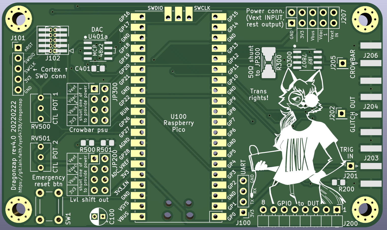
Front

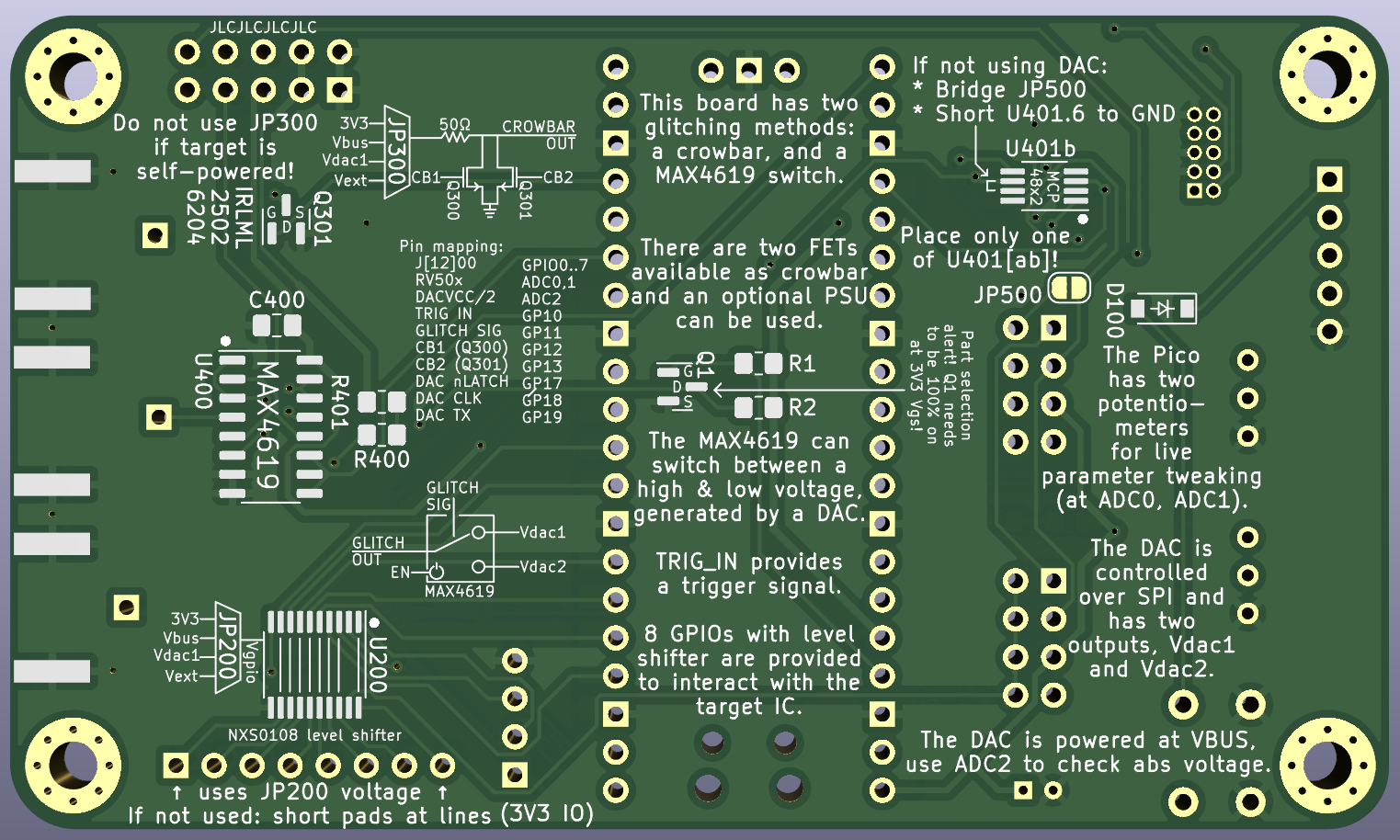
Back

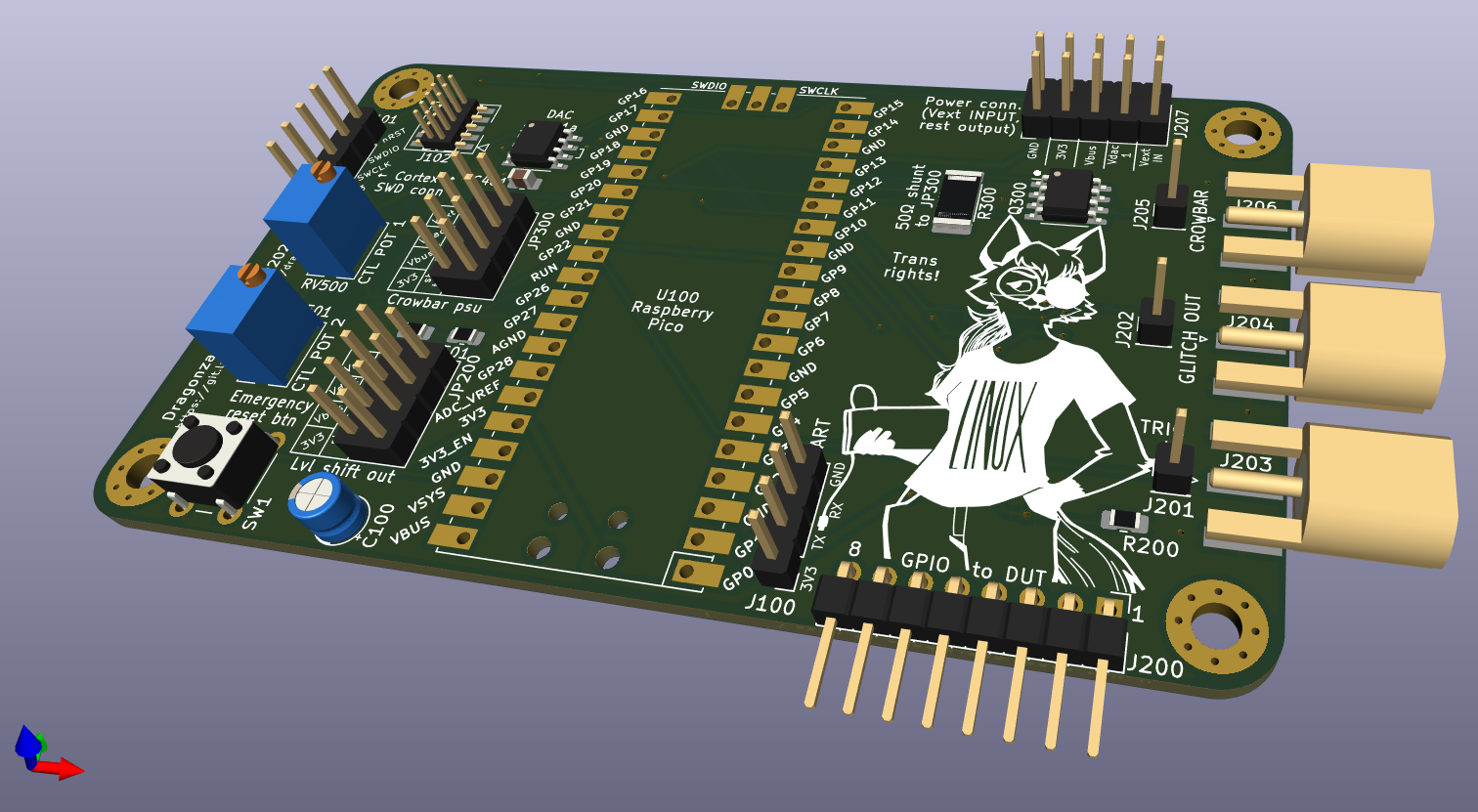
3D view, with components

Notes
External module and footprint sources:
Usage
Firmware of the Pico controller is still TODO. Most of the documentation can
be found on the PCB silkscreen.
Pico pinout
| Name |
Pico pin |
Usage |
| DUT GPIO |
GP0..GP7 |
Generic GPIO to the target DUT, goes through level shifter U200 and out to J200. GP0 and GP1 are also connected to JP100 for UART. |
| RV50x |
ADC0, ADC1 |
Potentiometers that can be used for manual parameter tweaking. |
| DACVCC/2 |
ADC2 |
Can be used to calculate the maximum voltage the DAC can reach, for calibration. |
| TRIG IN |
GP10 |
DUT trigger input. |
| GLITCH SIG |
GP11 |
DUT glitch (voltage supply) output, from U400. |
| CB1 (Q300) |
GP12 |
Crowbar gate 1 |
| CB2 (Q301) |
GP13 |
Crowbar gate 2 |
| DAC nLATCH |
GP17 |
nLATCH signal of the MCP4802 DAC (U401). |
| DAC CLK |
GP18 |
SPI clock signal of U401. |
| DAC TX |
GP19 |
SPI controller-to-device data signal of U401. |
BOM
Base components
| Ref |
Quantity |
Product |
Footprint |
Description |
Notes |
| U100 |
1 |
Raspberry Pico |
Pico module |
Raspberry Pico module/board |
This one serves as the glitch controller. Very important. |
| C100 |
1 |
47 uF |
THT Radial P2.00mm |
Electrolytic capacitor |
Extra decoupling capacitor for the Pico. |
| J200 |
1 |
Pin header 01x08 |
THT 2.54mm 01x08 |
Generic pin header |
Main GPIO to DUT connector, goes through level shifter U200. |
| J201, J202, J205 |
3 |
Pin header 01x01 |
THT 2.54mm 01x01 |
Generic pin header |
Main glitching to DUT connectors (pin headers). |
| J203, J204, J206 |
3 |
Amphenol 132289 |
SMA edge-mount connector |
SMA connector |
Main glitching to DUT connectors (SMA connectors). Has many other compatible connectors. |
Optional connectors
| Ref |
Quantity |
Product |
Footprint |
Description |
Notes |
| J207 |
1 |
Pin header 02x05 |
THT 2.54mm 02x05 |
Generic pin header |
Power out (and extra external voltage in) connector. |
| D100 |
1 |
1N4001 |
SOD-123 |
Generic or Schottky diode. |
Reset diode for external reset signal (SWD). |
| J100 |
1 |
Pin header 01x04 |
THT 2.54mm 01x04 |
Generic pin header |
UART connector (nonstandard, 2.54mm jumper) |
| J101 |
1 |
Pin header 01x05 |
THT 2.54mm 01x05 |
Generic pin header |
SWD connector (nonstandard, 2.54mm jumper) |
| J102 |
1 |
FTSH-105-01-L-DV-007-K |
THT 1.27mm 02x05 -OR- FTSH-105 SMD |
Cortex debug connector |
SWD connector (standard FTSH connector, 1.27mm pitch, either through-hole or surface-mount) |
Manual control potentiometers
| Ref |
Quantity |
Product |
Footprint |
Description |
Notes |
| RV500, RV501 |
2 |
Potentiometer |
THT 2.54mm 1x3 |
Potentiometer with colinear leads. |
Used for optional manual control of parameters. |
If you need the "emergency reset button"
| Ref |
Quantity |
Product |
Footprint |
Description |
Notes |
| Q1 |
1 |
Generic NMOS |
SOT-23 (GSD) |
N-MOSFET transistor |
Make sure it is completely on at a Vgs of 3.3V! Invertor NMOS for reset signal. |
| SW1 |
1 |
Push button |
THT 4-lead 6x6mm |
Two-by-two push button switch, generic |
Make sure the bends in the pushbutton leads are parallell with the lines on the silkscreen. |
| R1, R2 |
2 |
220k |
0805 |
Resistor |
Pullup/pulldown resistors. |
The emergency reset button will stop U100, and disable most other ICs (eg. U400, U200).
If you need the DAC
The DAC can be used for the level shifter, crowbar glitcher and SPDT glitcher
(selected using JP200, JP300 and JP500).
| Ref |
Quantity |
Product |
Footprint |
Description |
Notes |
| U401 |
1 |
MCP4802 |
SOIC-8 3.9x4.9 (U401a) -OR- MSOP-8 3x3mm P0.65mm (U401b) |
2-channel 8-bit DAC, SPI interface. |
DAC, optional. If not placed, you probably want to short JP500, and short the two leads as indicated on the silkscreen. SOIC and MSOP both work. |
| R500, R501 |
2 |
220k |
0805 |
Generic resistor |
Voltage divider for max voltage sensing of U401. Only needed if you place the DAC (U401). |
| C401 |
1 |
10 nF |
0805 |
Unpolarized (MLCC) capacitor |
Decoupling capacitor for U401. Optional. |
If you need the level shifter
| Ref |
Quantity |
Product |
Footprint |
Description |
Notes |
| U200 |
1 |
TXS0108EPW -OR- NXS0108PW |
TSSOP-20 4.4x6.5mm P0.65mm |
Bidirectional level-shifting voltage translator |
The level shifter. Source from TI or Nexperia. |
| R200 |
1 |
47k |
0805 |
Pulldown resistor |
Used for the enable line of U200. |
| JP200 |
1 |
Pin header 02x04 |
THT 2.54mm 02x04 |
Level shifter external voltage selector. |
Place a generic pin header here, use a pin shunt to select the voltage. |
If not using the level shifter, short the leads of the footprint of U200 as
shown on the PCB silkscreen.
If you need the crowbar glitching circuit
| Ref |
Quantity |
Product |
Footprint |
Description |
Notes |
| Q300 |
1 |
IRF7807/Si4850BDY/Si3463BDY |
SOIC-8 3.9x4.9mm |
N-channel Power MOSFET, SO-8 |
Slower but higher-duty (current-wise) crowbar MOSFET. Need not be placed if Q301 is present. |
| Q301 |
1 |
IRLML2502/IRLML6204 |
SOT-23 |
N-channel MOSFET, SOT-23 |
Faster but more fragile crowbar MOSFET. Need not be placed if Q300 is present. |
| R300 |
1 |
50 Ohm |
0805/1206/2010/2512 |
Current limiting resistor |
Current limit resistor through which power is optionally supplied to the target. Several footprints work. Use eg. ESR10EZPF49R9. |
| JP300 |
1 |
Pin header 02x04 |
THT 2.43mm 02x04 |
Generic pin header |
Crowbar power supply, place generic pin header and use a pin shunt. Can be left open if target is self-powered. |
Note, Q300 and Q301 are selected by separate GPIO lines on the Pico.
If you need the SPDT switch glitching circuit
| Ref |
Quantity |
Product |
Footprint |
Description |
Notes |
| U400 |
1 |
MAX4619CSE+ |
SOIC-8 3.9x4.9mm |
Triple analog SPDT switch |
Fast SPDT switch IC, used for glitching (selecting between high and low voltage levels). |
| R400, R401 |
2 |
220k |
0805 |
Generic resistor |
Pullup/pulldown resistors for the enable line of U400. |
| C400 |
1 |
10 nF |
0805 |
Unpolarized (MLCC) capacitor |
Decoupling capacitor for U400. Optional. |
